هل توجد معلومة عن دقة التصنيع nm؟
بعض بحوث KACST تصل الى 100NM
The firm, based on Los Angeles, is a spinout from the Center of Excellence for Green Nanotechnologies at UCLA and King Abdulaziz City for Science and Technology (KACST).
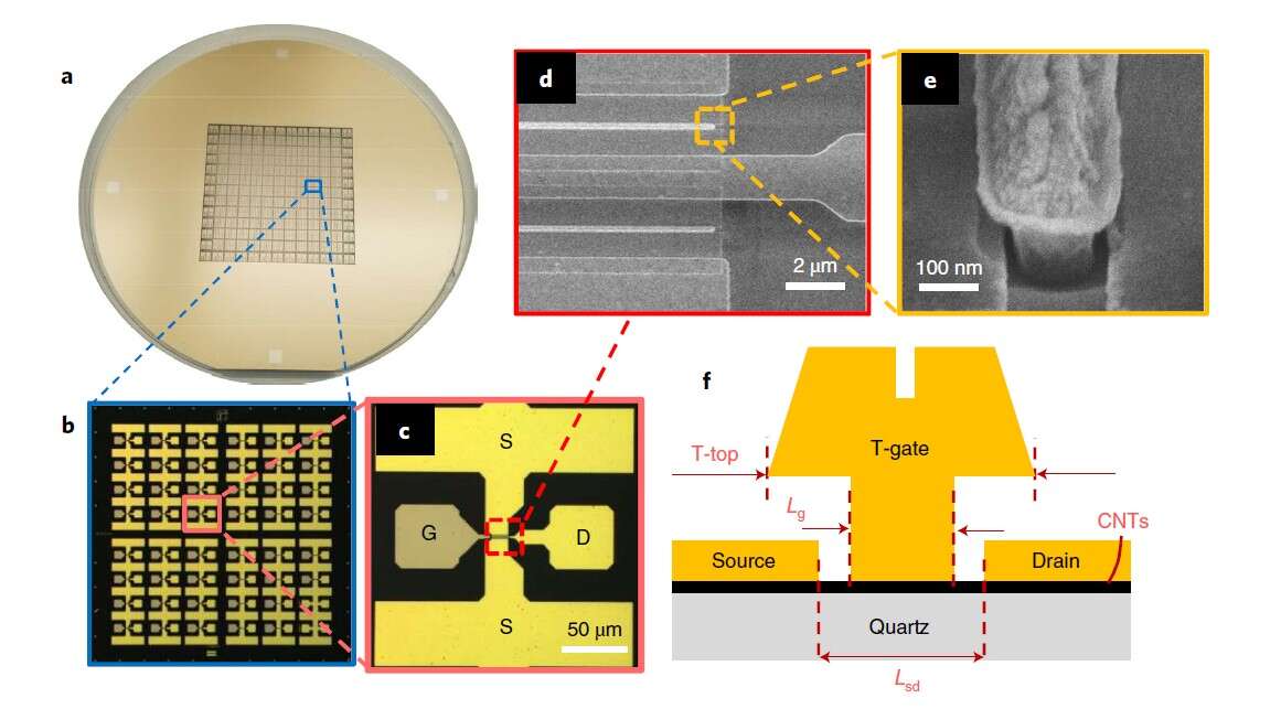
The paper reports the wafer-scalable fabrication of an array of aligned carbon nanotube field-effect transistors operating at gigahertz frequencies. The devices have gate lengths of 110 nm and are capable, in distinct devices, of an extrinsic cutoff frequency and maximum frequency of oscillation of over 100 GHz, which surpasses the 90 GHz cutoff frequency of radio-frequency CMOS devices with gate lengths of 100 nm and is close to the performance of GaAs technology.
The paper reports the wafer-scalable fabrication of an array of aligned carbon nanotube field-effect transistors operating at gigahertz frequencies. The devices have gate lengths of 110 nm and are capable, in distinct devices, of an extrinsic cutoff frequency and maximum frequency of oscillation of over 100 GHz, which surpasses the 90 GHz cutoff frequency of radio-frequency CMOS devices with gate lengths of 100 nm and is close to the performance of GaAs technology.