
شغل جبار
بالتوفيق للمملكة
بالتوفيق للمملكة

قم بمتابعة الفيديو أدناه لمعرفة كيفية تثبيت موقعنا كتطبيق ويب على الشاشة الرئيسية.
ملاحظة: قد لا تكون هذه الميزة متاحة في بعض المتصفحات.
شيئ ممتاز هذه الرقاقات تستعمل في اغلب الصناعات الالكترونية ، و عليها طلب كبير لدرجة شركات تتوقف ايام كل شهر نظير النقص الكبير في هذه الرقاقات ، شركات على اصابع اليد هي الرائدة في صناعة هذه الرقاقات ، ثلاث اشياء يجب توافرها ستأخد حينها السعودية مكانا في هذه الصناعة (الجودة ، التكلفة ، التقنية المستعملة )
بس مشكلته انه يخترق الخصوصية. يتطلب تتبع مستمر للفرداللي فهمته ان مصمم تطبيق توكلنا كان خريج احد دوراتهم
والله عظيم جداا جداا
ماشاء الله تبارك الله
عمار ياوطني ....
طيب هل نقدر نسوي مواقع مستقلة للوطن العربي مثل تويتر واتساب جوجل يوتيوب الخ الخ الخ
لكي نستقل عن الغرب؟
موجود محركات بحث عربية على أرض الواقعطيب هل نقدر نسوي مواقع مستقلة للوطن العربي مثل تويتر واتساب جوجل يوتيوب الخ الخ الخ
لكي نستقل عن الغرب؟
لا يوجد شيء اسمه مستحيل أمام البشر بشكل عام و بشكل خاص أمام الشعب السعوديمنافسه تايوان بكره مستحيله
بس مشكلته انه يخترق الخصوصية. يتطلب تتبع مستمر للفرد
")
هل من الممكن أن توضح لنا ما نوع الرقائق التي يتكلم عنها السواحة؟ اكثر ٦٠ الف ضعف من رحلة القمر يعني انها بمواصفات رديئة. في ذلك الوقت لم يكن هناك كمبيوتر ولا رقائق بل كانت ايام ترانزستر.محمد السويد حمار ما يفهم كعادته سبحان الله.
المقصود ليس رقاقة سيليكون عادية او بمواصفات وبنية تخص منتج اجنبي بل سعودية البناء من الصفر يعني من الground zero.
لكن انصحك تراجع نفسك بخصوص الحمار اللي اسمه محمد السويد. ايضا نصيحة لا تثق بأي شخص صورته مثل صورة بروفايل محمد السويد. يبي يعطيك انطباع انه فاهم وبحركة صوروني وانا مدري يعنني لقطة عارضة له وهو يتكلم
طيب هل نقدر نسوي مواقع مستقلة للوطن العربي مثل تويتر واتساب جوجل يوتيوب الخ الخ الخ
لكي نستقل عن الغرب؟
 من جدك
لا برجليها ولا بيديها ... متصنعهاش خالصهي باقي الدول بتصنعها برجليها ولا ايه

لا اعلم ما دخل هذا المحتوى بكلام الوزير. ما اقتبسته يتكلم عن مشاريع بحثية تقوم بها المدينة مع باحثين خارجين لتصميم شرائح إلكترونية. كلام الوزير يتكلم عن إنتاج شريحة الكثرونية بمواصفات عالمية.
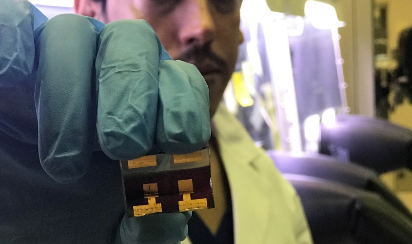
A deep insight into perovskite solar cellsResearchers examine which components influence the performance and stability of these promising materials.
Cheap, flexible, and efficient, perovskite solar cells are the rising star in the field of photovoltaics. However, their low durability has kept them from the consumer market.
But now, KACST researchers, in collaboration with École Polytechnique Fédérale de Lausanne, Switzerland, have unravelled some fundamental electronic processes, which could be useful to improve the performance of these light-harvesting devices.
The researchers tested and compared two types of perovskites. The perovskites general formula is ABX3, where A is a larger cation (positively charged ion), B a smaller metallic cation, and X a halide anion (a halogen atom that is negatively charged). The team used a frame of lead bromide with either formamidinium (FA) or caesium (Cs) as A-site cations, creating FAPbBr3 and CsPbBr3, respectively.
“Stability is still an issue in perovskite solar cells, particularly in humid and hot conditions. We used a frame of lead bromide, because it has higher stability compared to others, such as lead iodide. Then, we thought that optimizing the A cation could further improve the efficiency of these devices,” says Mohammad Hayal Alotaibi, assistant professor at the Materials Science Research Institute, and a member of the team. “The size of A cations can play an important role. For example, if they do not fit properly in their positions, they may cause poor functioning.”
Compared to the cell made with caesium (CsPbBr3), the cell made with formamidinium (FAPbBr3) has more favourable photocurrent, photovoltage, and fill factor: three photovoltaic parameters that determine the power conversion efficiency of a solar cell.
Perovskite solar cells were built in layers, starting with fluorine doped tin oxide glass, followed by titanium dioxide (TiO2), perovskite, then spiro-OMeTAD as hole transport material (HTM) and finally gold. Photons of the sunlight are absorbed by the perovskite film, where they excite some electrons and cause them to migrate to the TiO2 layer. A hole is created where each electron was formerly bound. This hole also participates in conduction by moving to the HTM. The scientists used various techniques to measure how free electrons roam within the device, to generate current, and end their journey by recombining with the holes.
Several analyses confirmed that electrons in devices made with formamidinium can move quicker across the TiO2-perovskite interface, than in those made with caesium. The devices of caesium are more subject to power loss as they have higher internal resistances for charge transport, and lower shunt resistance, which provides an alternate current path for the light-generated current. Caesium cells are also limited by mechanisms that facilitate a quicker recombination between electrons and holes.
The team is planning to introduce other A cations of various sizes, as well as different anions.
في موضوع |
|---|
فقط الحاسبات "فيليكس" ولاحقا الحاسبات الميكانيكية "مرسيدس" [تم] استخدامها للحسابات


 الرياضيات في خدمة السلاح النووي